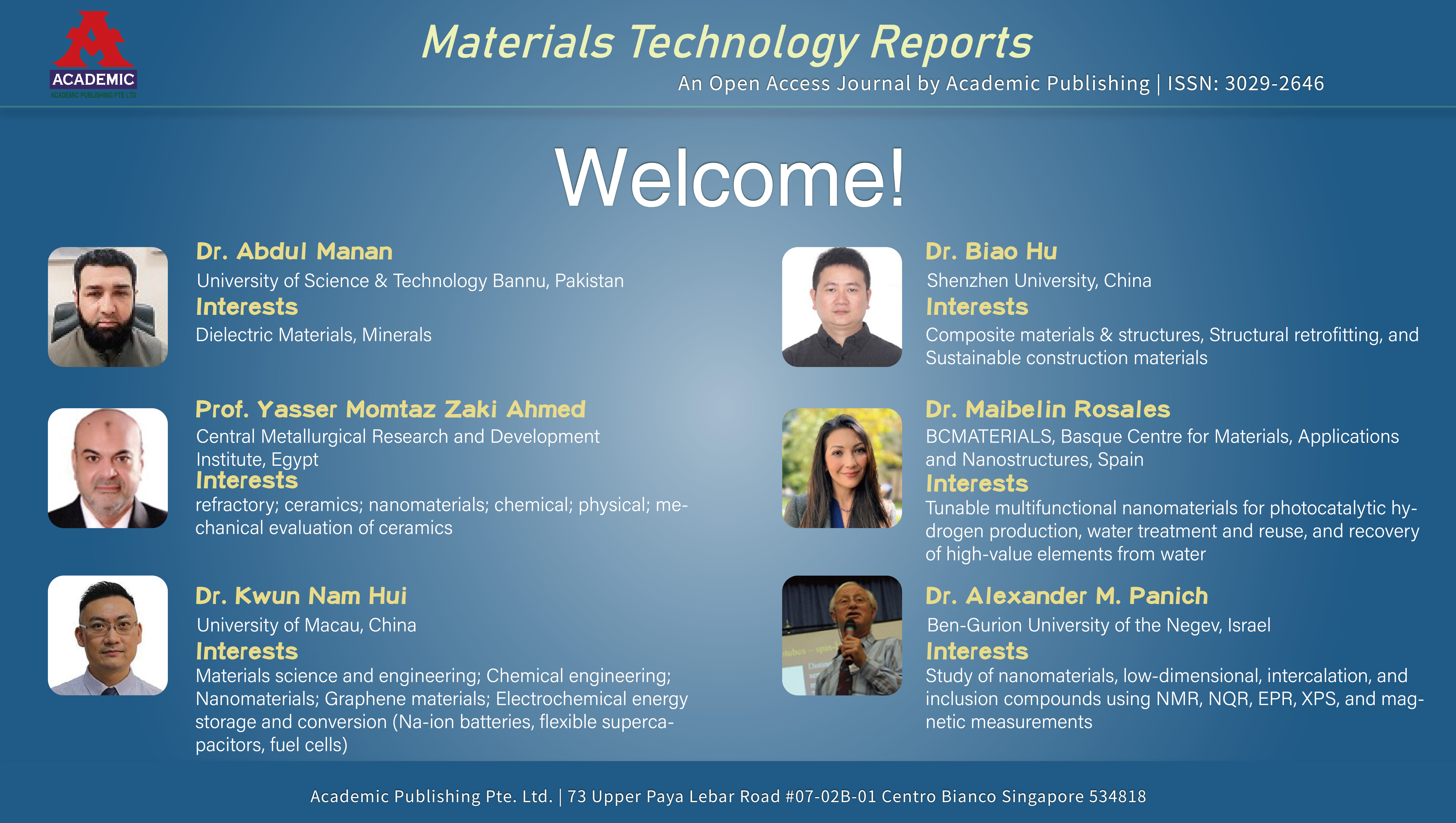
Welcome to the New Editorial Board Members!
2024-11-25


Materials Technology Reports (MTR) is an open access journal of related scientific research and technology development. It provides a forum for the publication of reviews, regular research papers (articles), and short communications on fundamental science, engineering, and practical applications of materials. Our aim is to encourage scientists to publish their experimental and theoretical results in great detail. Therefore, there is no restriction on the length of the papers. The full experimental details must be provided so that the results can be reproduced.
 Open Access
Review
Article ID: 4242
by Miyi Duan, Jiali Wei, Jingtong Zhang
Materials Technology Reports, Vol.4, No.2, 2026;
Due to their broad coverage and long operational duration, as well as their ability to be used as quasi-stationary platforms, stratospheric airships have gained increasing popularity for persistent near-space communication relay, Earth observation, environmental monitoring, and military reconnaissance. Nevertheless, their operational stability is severely threatened by the harsh conditions of the stratosphere, including intense ultraviolet light, ozone exposure, low pressure, extreme temperature variations, and periodic mechanical strain. The envelope coating, as the primary discontinuity between the lifting gas and the external environment, is a determinant of structural integrity, gas retention, thermal control, and operational reliability. This review is a systematic summary of recent developments in intelligent nanocomposite coating materials for airships operating in stratospheric airspace. The practical needs of these coatings, such as mechanical strength, environmental stability, gas protection properties, light structures, and multifunctionality, are initially discussed. Next, representative polymer matrices, multifunctional nanofillers, and new fabrication technologies are presented, with a focus on interface engineering and hierarchical structure design. The smart capabilities of self-healing, self-sensing, stimuli-responsive adaptation, and synergistic performance improvement mechanisms have been extensively examined. Existing uses in envelope protection, thermal control, anti-icing, anti-static dissipation, and structural health monitoring are outlined, and issues related to scalability, durability, cost, and system integration are noted. Lastly, future development trends, including AI-aided materials design, digital twins, self-powered sensing systems, and sustainable multifunctional coatings, are suggested. The intelligent nanocomposite coating is anticipated to transform the development of stratospheric airships by enabling the creation of lightweight, adaptive, and autonomous near-space systems.
Open Access
Article
Article ID: 4049
by Ahmad Reza Rastkar, Taha Shariati
Materials Technology Reports, Vol.4, No.1, 2026;
Ni superalloys are mostly used in turbine engines. But they suffer from high temperature oxidation. So, many investigations have been tried to protect the surface of these materials by pack aluminizing. A plasma paste process was used to aluminize the surface of superalloy IN-738. Nickel aluminum phases were created on the surface of the nickel-based superalloy IN-738 by plasma paste aluminizing with pure aluminum and Al-Si mixtures. Specimens were plasma-paste aluminized at 750–900 ºC for 1 h in low pressures of 10 mbar argon gas without Si and with 5–10% Si. Microstructural and compositional evaluations were studied using optical and scanning electron microscopes, EDS, X-ray diffraction (XRD) techniques, and Vickers microhardness tests. A mixture of fine or coarse equiaxed-grained microstructure of NiAl, Ni2Al3 with precipitates of Al4Cr phases were observed in the coating layers. The addition of silicon showed the transformation of the NiAl and Ni2Al3 phases in the compound layers from fine-grained structures to nearly coarse equiaxed grains. In this plasma paste process, the silicon can be dissolved in the coating up to 10 at.% of the total coating composition and is mostly concentrated in some phases. Average Vickers microhardness analysis across the transverse cross section of aluminized samples under 500 g force revealed mostly an increase in hardness from approximately 250–300 HV0.5 in the substrate to 550–600 HV0.5 in the coating layers.
Open Access
Article
Article ID: 3996
by Fareenpoornima Rafiq, Sumathi Jones, Parthipan Govindsamy, Papitha Purushothaman
Materials Technology Reports, Vol.4, No.1, 2026;
The research reports first on the optical properties of BaCoO2.6 nanoparticles, using the transmission spectrum, viz., the band gap. The nanoparticle size of 25 nm with grain size ranging from 0.5 μm to 5 μm was revealed. Tauc's indirect transition model describes the optical band gap (Eg) as 5.28 eV, using which the optical features such as extinction coefficient, refractive index, and the loss function have been evaluated. The synthesized sample's average refractive index lies in the range 1.0–2.5, the Urbach energy, calculated from inter-band localized electronic states generated by defects, was found to be 2.01 eV. As the entire region does not bear any absorption band, the sample finds its suitability in NLO-SHG devices. Interesting outcomes in line with optical properties were also demonstrated by the photoluminescence properties. The electron transition at 800 nm, which is also linked to the electronic transition of Co2+/Co3+ ions, is responsible for the peak. The electrons may be trapped at the oxygen vacancies at a tetrahedral site, or they may be caused by impurities or structural flaws in the material and may suggest a mixed phase transition. The magnetic squareness ratio being less than 0.5 emphasizes the synthesized sample’s anisotropic, single-domain, soft magnetic nature. The present exploration of BaCoO2.6 nanoparticles highlights that their antimicrobial efficacy extends well beyond conventional growth inhibition metrics such as the minimum inhibitory concentration (MIC) and the minimum bactericidal concentration (MBC).
Open Access
Review
Article ID: 4042
by Salaman Ahamad, Shaista Fatima, Sameera Zafar, Mohd Hasan Mujahid
Materials Technology Reports, Vol.4, No.1, 2026;
Nanomaterials have been found to possess tremendous potential as novel enabling elements in the highly dynamic field of flexible wearable bioelectronics. This is owing to their ability to allow for smooth interfacing between artificially designed devices and complex biological systems at both the molecular and cellular levels. Their highly desirable physicochemical properties, including elevated surface-area-to-volume ratios, quantum confinement, electronic conductivity, and mechanical flexibility, make nanomaterials promising candidates for novel wearable electronic devices that can find applications in continuous biosensing, bioactuation, neural interfacing, and real-time bioimaging. Most importantly, they can allow for the realization of basic elements of bioelectronics, such as bio-memory devices, biological logic gates, and biomolecule-integrated processors. These can potentially allow for overcoming the limitations of conventional rigid silicon-based electronic devices through intelligent integration with biomolecular recognition. This review article presents a systematic and comprehensive discussion on the most prominent classes of engineered nanomaterials utilized in the development of flexible wearable bioelectronics, including carbon-based nanostructured materials, intrinsically conducting polymers, metallic and bimetallic nanomaterials, as well as multifunctional nanocomposites. In addition, the review article places significant emphasis on the elucidation of the most significant structure-function relationships in the context of the most prominent application areas, including epidermal biosensing devices, soft neural interfaces, as well as biomimetic tissue engineering constructs. In addition, the most promising trends in the development of flexible, stretchable, as well as skin-conformable bioelectronic architectures are also critically discussed in the article. The current challenges in the development of flexible wearable bioelectronics, including the most prominent issues in the context of biocompatibility, long-term stability, and scalability, are also discussed in the article.
Open Access
Article
Article ID: 4128
by Shijing Wang, Mingyu Zhang, Jie Liang, Leyi Tu, Jian Li, Zhiqian Gui, Jiale Zhu, Qian Wu, Deqin He, Haixin Qiu, Zhaoxiang Wang
Materials Technology Reports, Vol.4, No.1, 2026;
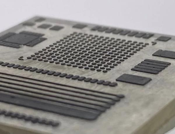
In this study, various silicon carbide (SiC) trench and via pattern etching processes are investigated, and high-aspect-ratio super-junction (SJ) structures are successfully fabricated. SiC SJ trenches are promising for ultra-high-voltage power device applications. Using a SiO₂ hard mask, SiC trenches with aspect ratios from 3:1 to 15:1 and depths exceeding 21 μm are prepared. Etch selectivity (SiC/SiO₂) is calculated based on the etched thicknesses of SiC and SiO₂ under the same process, and the selectivity can exceed 10:1 by optimizing hardware configuration and process parameters, especially gas combination and equipment settings. The significant effect of sidewall roughness transfers from the oxide hard mask to the SiC substrate is revealed. A smooth and optimized oxide hard mask sidewall is the key to reducing the final SiC sidewall roughness during pattern transfer. Full-wafer uniformity is improved by multiple tuning methods, including power ratio split, gas ratio split, temperature distribution control, and refined process parameters. Excellent uniformity is achieved: SiC trench critical dimension (CD) variation below 2%, SiC etch depth uniformity below 1%, and sidewall angles above 88° across the entire wafer. Long-term tool stability is verified over 10 consecutive months of etch rate monitoring with standard monitor wafers. The etch rate variation is controlled within 3% and uniformity below 2%, demonstrating reliable mass-production manufacturability of the SiC trench process.
Open Access
Review
Article ID: 4107
by Xiaoling Wu, Manni Liang, Ruiqing Su, Shui He, Jieyi Yang, Xingyuan Gao
Materials Technology Reports, Vol.4, No.1, 2026;
Carbon-based electrochemical adsorption technology has become an increasingly important method in the field of advanced water pollution treatment, and it is expected to provide critical technical support for water environmental restoration and drinking water safety. Traditional water treatment technologies have obvious limitations, such as poor selectivity, high energy consumption, difficulty in material regeneration, and the risk of secondary pollution. In this context, it is crucial to develop new water treatment technologies that are efficient, stable, low-consumption, and environmentally friendly. Carbon-based electrochemical adsorption technology makes full use of the superior electrical conductivity, high specific surface area, tunable surface chemistry, and relatively low cost of carbon materials, showing great potential in water pollution control. This paper systematically reviews carbon-based electrochemical adsorption technology, summarizes key adsorption materials, removal mechanisms for various pollutants, optimization strategies related to system configuration and operating parameters, and the latest application developments in different water treatment fields. The article clearly distinguishes the roles of non-Faradaic (capacitive) processes based on double-layer charging and Faradaic processes involving electron transfer in pollutant enrichment and transformation, constructing a clear mechanistic framework. Furthermore, the paper critically analyzes the main challenges faced by this technology, including the synergistic optimization of material performance, in-depth analysis of interfacial mechanisms, the complexity of actual water bodies, system-scale application, and long-term operational stability, and proposes future research directions to promote its engineering and large-scale application.

University of Chile, Chile
CAS
Google Scholar
J-Gate
All the publications will be archived by the PKP Preservation Network for long-term electronic preservation.
Authors are encouraged to self-archive the final version of their published articles into institutional repositories (such as those listed in the Directory of Open Access Repositories).
Authors are also encouraged to use the final PDF version published on the website of Academic Publishing.

Academic Publishing insists on taking academic exchange and publication as the main line, carrying out comprehensive management based on science and technology, and fully exploring excellent international publishing resources. Within 5 years, it will form a strategic framework and scale with science (S), technology (T), medicine (M), education (E), and humanities and arts (H) as the main publishing fields. Academic Publishing is headquartered in Singapore and based in Malaysia, with the United States and China providing the main scientific and academic resources. At the same time, it has established long-term good cooperative relations with other publishing companies, scientific research communities, and academic organizations in more than a dozen countries and regions. Academic Publishing uses English and Chinese as its main publishing languages, mainly publishing books, journals, and conference papers in print and online. The vast majority of publications follow the international open access policy, providing stable and long-term quality and professional publications. With the joint efforts of the expert team and our professional editorial team, our publications will gradually be indexed by international databases in stages to provide convenient and professional retrieval for various scholars. At the same time, manuscripts we accept will be subject to the peer review principle, and cutting-edge and innovative research articles will be preferentially accepted for peer reference and discussion. All kinds of our publications are welcome for peer to contribute, access, and download
 73 Upper Paya Lebar Road #07-02B-01 Centro Bianco Singapore 534818
 editorial_office@acad-pub.com